
Switching strategies for increasing processor power efficiency
May 01, 2008
Story

Designers can employ several techniques that greatly improve efficiency in switching power supplies and make switching regulators feasible in differen...
Continual advancements in smaller silicon geometries have enabled lower operating voltages in embedded devices, particularly microprocessors. Operating voltages for processor cores are now as low as 1.2 V and quickly moving to 0.8 V, presenting a challenge as to how designers can efficiently power these devices. As opposed to the traditional method of using linear regulators to power low-voltage devices, using switching regulators in these applications can help solve this problem. Depending on system requirements, designers can use various architectures to maximize switching regulators’ efficiency.
A typical low-power embedded processor draws 300-600 mA. Using a switching regulator in older-generation processors where core voltages were 3.3 V provided little benefit. However, decreasing core voltages are presenting a significant opportunity for efficiency improvements, especially when powered by a lithium ion cell (4.2 V) or 5 V rail. For example, a linear regulator in a 4.2 V system will waste 1.8 W [(4.2-1.2 V) x 600 mA] when regulating down to 1.2 V. In contrast, a switching regulator can perform with up to 95 percent efficiency under the same conditions, which can add a significant amount of operation time to the system.
The potential noise created by a switching regulator, its inefficiency at light loads, and the need for more complex control have traditionally discouraged designers from using this type of regulator for an embedded processor. Additionally, linear regulators’ larger footprint has made linear regulation the preferred method. Nonetheless, designers can employ several techniques that greatly improve efficiency in switching power supplies and make switching regulators feasible in different types of designs. Single ICs with an integrated controller, pass devices, and compensation components have made switching regulators less design-intensive and more cost-effective to implement.
Standard buck topology
A simple buck switcher comprises a Field-Effect Transistor (FET), diode, inductor, capacitor, and controller, as shown in Figure 1. Regulating output voltage in this topology involves varying the duty cycle on the FET’s gate to increase or decrease current through the inductor, a method referred to as Pulse Width Modulation (PWM). A PWM switching regulator’s efficiency can be upwards of 95 percent when operated at full load. However, when operated at light load, a switching regulator’s efficiency drops off significantly, making it undesirable for systems that operate under changing load conditions or require low current or sleep modes.
|
|

To overcome a switching regulator’s inefficiency during light load conditions, designers can put the regulator in pulse skipping or Pulse Frequency Modulation (PFM) mode. When in PFM mode, the FET in the switching regulator only operates when output voltage falls below the low limit. This reduces the number of pulses, which in turn reduces switching losses through the FET, inductor, and diode, thus improving efficiency under light load conditions. For the device shown in Figure 2, the regulator transitions from PFM to PWM at about 100 mA, thereby maximizing efficiency throughout the entire range of output currents.
|
|

When designing with a PFM regulator, designers must take into account the applications in which it will be used. Since the switcher’s frequency varies with the output load, it is possible that switching frequency can fall as low as the audio band, which can produce undesirable noise problems. Fortunately, certain tools available in the market today can ensure that frequency never enters the audio band. Although these tools may cause a slight decrease in efficiency under light loads, they can save designers countless hours spent eliminating a noise issue.
Synchronous topology
Designers can make additional improvements to a switcher’s efficiency using a synchronous topology, as shown in Figure 3. This topology can reduce switching losses and reverse recovery losses through the diode by replacing the diode with a low Rds(on) FET.
|
|
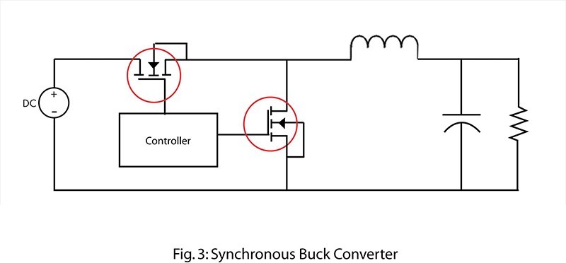
In this topology, the timing of synchronous switching is critical. If both FETs are conducting, power will be lost on every cycle and efficiency will be compromised. In addition, designers must consider which devices to choose. For example, the FET’s gate capacitance is an important variable because it can keep the low side FET in conduction after the controller has switched off the FET. During the short period of time that the gate remains charged, the input power is shunted directly to ground. The Rds(on) and FETs’ gate capacitance will have the greatest impact on efficiency in this topology; thus, it is important to optimize both.
In the aforementioned topologies, using higher switching frequencies can be advantageous when board space is very limited. Higher switching frequencies allow designers to use smaller passive components such as the inductor and output capacitor, which can decrease the design’s cost and overall footprint. However, this comes at the price of decreased efficiency. When frequency increases, the number of times that FETs switch increases, which in turn increases losses. In addition, the smaller inductor and capacitor will likely create higher ripple on output voltage.
Multiphase topology
To overcome today’s stringent ripple requirements while maintaining efficiency in embedded designs, designers can use multiphase DC-DC switchers. This topology can reduce switching losses while effectively increasing the regulator’s switching frequency.
For example, consider a single-phase DC-DC synchronous switcher connected to a load, Iload. Switching losses through each FET are I2R or Iload2* Rds(on). In a multiphase design, switching losses are the same through each FET. However, the current in each phase is divided by the number of phases. Therefore, switching losses in a two-phase design can be reduced by:
|
|

or, in general:
|
|

where N is the number of phases in the design.
Additionally, a multiphase design improves the regulator’s ripple currents and transient response time. This comes at an increase in cost and footprint because an inductor and two FETs must be added for each phase and because the controller becomes larger and more complex.
Narrowing the options
Power efficiency is the key to meeting the demand for extended battery life in portable products. Processor manufacturers have aided this effort by reducing operating voltages, but power supplies must adapt to maximize efficiency. When deciding on the most efficient power supply, it is important to examine the variables to assure the power supply will meet processor requirements. Power supply cost must be part of the decision as well.
The standard buck switcher provides efficiency when operating in a PWM mode and is less complex than the synchronous buck, making it a less expensive option. However, the diode creates a voltage drop, which wastes some power. The synchronous buck reduces this voltage drop using a FET in place of the diode, which increases efficiency but at higher cost.
The multimode regulator provides efficiency improvements over the full load range by switching from PWM to PFM when the processor is in sleep mode. This adds some output ripple voltage, but as long as it stays within the processor’s power specification, it will significantly improve battery life. The multiphase regulator maintains efficiency while eliminating much of the output ripple voltage, also at higher cost.
Designers can follow these guidelines when designing power supplies for an embedded processor. All designs require trade-offs, and power supplies are no exception. Given the budget constraints, power requirements, and efficiency target for any design, these strategies will help narrow the options to identify a power supply that provides the best compromise of all three.
Fairchild Semiconductor
207-775-8100
[email protected]
[email protected]
www.fairchildsemi.com


