Passive IR sensor front-end design
September 01, 2014

Conventional passive infrared (PIR) sensor application circuits contain numerous bulky passive components. Shrinking the electronics down to the size...
Low-cost pyroelectric sensors find use in occupant detection and remote monitoring of heat sources. They consist of a ceramic crystal that’s locally buffered by a JFET preamp that gets its drain current bias through an external load resistor.
The change in output voltage with incident IR is very small (~3.6 mV peak-to-peak, for the Murata sensor used to prototype the system) compared to the sensor’s inherent offset voltage (more than 1,800 mV for a 5 V excitation). The offset voltage is highly sensitive to temperature. Therefore the interface circuitry has to differentiate between the variations in this offset voltage and the actual sensor output corresponding to a motion. The interfacing circuitry has its work cut out for it, as the signal corresponding to a motion is often less than 0.2 percent of the offset voltage.
The datasheets of PIR sensors usually show various distinct application circuits for different modes of operation. These circuits require significant numbers of bulky external passive and active components to filter out the low frequency offset voltage. The circuits provide a broad bandpass response to the AC signal coming from the buffered output of the sensor element. DC and extremely low frequency signals are suppressed by the highpass portion of the response, with cutoff frequencies often below 0.01 Hz, resulting in settling and recovery times measured in minutes! At the upper end, frequencies above about 50 Hz are suppressed, generally with a two-pole response (not by enough to cope with large amounts of AC line frequency modulation, though). The mid-band gain applied to the signals that do get through is anything from 10,000 to 40,000!
The PSoC system in Figure 1 uses a hybrid (analog-plus-digital) servo loop to remove the DC offset, resulting in a low-cost single chip solution that consumes far less area and volume, and can be integrated within a small sensor unit. This integrated sensor-plus-SoC package, the same size as a standalone sensor, can give high analog output levels, digital outputs (including LED drivers), and host connectivity options such as UART, I2C, SPI, etc. Since many functions are performed in the digital domain, using firmware or programmable hardware, the SoC solution is highly flexible. The integrated SoC can be re-configured in the field to meet the requirements of the application. In addition, the parameters of the servo loop can be re-tuned using a host controller during runtime, to adapt to the changes in environment.
|
|
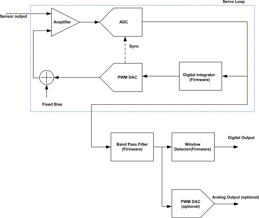
Figure 2 shows the implementation of the servo loop using the PSoC’s programmable analog and digital blocks. The start of conversion signal for the ADC is generated from the PWM output, using a frequency divider. This arrangement synchronizes the ADC conversion to the PWM servo feedback and reduces this noise component in the ADC output. The PWM runs at 5.8 kHz. The ADC sample rate is approximately 293 samples per second. In the servo loop circuit, Rpwm_1, Rpwm_2, and Cpwm form a T filter for the PWM output. Rg1 and Rg2 provide a DC bias that is close to the offset voltage of the PIR sensor. The PWM-filter circuit combination acts as a cost-effective, high-resolution 12-bit DAC.
|
|

The equivalent resistance from the inverting input of the Opamp to ground is close to 60 kΩ. Therefore, the gain of the non-inverting amplifier is approximately 113.
Mid- to high-frequency noise is controlled by a modest-sized capacitor connected across the feedback resistor to give a bandwidth of several hundred Hertz. This single gain stage is all that’s required, because the rest of the system sensitivity will come from the ADC stage that follows this. Using a single amplifier saves power, reduces cost, and improves the overload behaviour.
The non-inverting input to the amplifier has a capacitor to ground and a resistor to an I/O pin that is driven by a 12-bit PWM DAC whose input word comes from a digital integrator, which could be implemented either in firmware or in programmable digital hardware.
The Opamp output drives the inverting input of the SAR, whose non-inverting input goes to ground. This connection inverts the sense of the converter output. The SAR is converting at a rate of around 293 sps. The ADC’s aperture time can be left at the default setting, because the capacitor in the feedback loop rolls the closed loop gain off to unity well below the equivalent aperture frequency of the ADC.
The ADC output format is set to signed, so that an input voltage of 1.024 V (the reference voltage value) will result in a code of all zeroes at the ADC. The ADC drives the integrator, and when the loop is closed, the integrator output will move around to keep the mean value of the ADC code equal to zero. In other words, this process acts both as a highpass filter and as a working point stabilizer. It replaces the large capacitor value that would otherwise be needed to block the DC bias from the sensor. Because it’s implemented in code, it can easily be paused, reset, or sped up, meaning that the system can stabilize very quickly after power-up. This is a significant advantage over passive circuits relying on a large RC time constant.
As well as feeding the integrator, the ADC’s output data is applied to a first order IIR highpass filter at 0.005 Hz to 0.01 Hz, which eliminates any DC and low frequency information not completely suppressed by the servo loop. Following that, a suitable low pass filter blocks off whatever higher frequencies are considered undesirable, and extends the resolution of this stage well below the normal 12-bit resolution floor set by the ADC used here. At the sample rate involved, these filters can be implemented in the CPU. The overall response looks like a bandpass filter, obviously far more configurable in this digital implementation.
The amplifier, ADC, digital integrator, and the PWM DAC constitute a closed servo loop that removes the DC offset from the sensor output. When the sensor offset changes, the integrator accumulates the error signal and changes the amplifier bias via the PWM DAC, in such a way that the Opamp output (and the ADC count) is maintained at zero. Therefore, any change in offset is nullified. However, the change in sensor output corresponding to a motion will not be nullified because the servo loop is not fast enough to respond to sudden changes in sensor output. Typical frequency response of the servo loop is shown in Figure 3.
|
|

The filtered ADC value can be used in several ways. It can be compared against a threshold, and an alarm raised whenever the threshold is exceeded. It can be applied to timing circuits so that an alarm is only triggered when the level is exceeded by a preset time, and the alarm can then be stretched so that it lasts for a preset duration even when the stimulus disappears. Separate thresholds can be set for rising and falling values of signal. This allows the PIR sensor to discriminate between approaching and receding heat sources.
The digital output can also be converted back to a high-amplitude analog signal if required. The filtered ADC count data is appropriately scaled and applied to the input of another PWM block. The PWM signal is applied to a pin whose output is lowpass filtered by an RC filter and buffered using the other available Opamp in the SoC device chosen. This output can be passed to external circuitry as a replica of the input infrared variation irradiating the sensor.
The firmware flow of the project is shown in Figure 4. The firmware filters and integrators need to operate in real-time for the servo loop to work. Therefore, the firmware integrator and filters are included in the ADC interrupt service routine. Non-critical functions are in the outer loop in main.c.
|
|

In addition to running the servo loop and output routines, the firmware can send the data to a host controller for real-time monitoring, using the wide variety of communication blocks available in this modern programmable SoC, such as UART, I2C, SPI etc. The host can also re-tune the loop parameters during the runtime by sending commands back to the SoC.
Figure 5 shows a typical output of the system. The large variations in Wn indicate the detection of a motion. The filter coefficients and the threshold window can be adjusted during run-time. This is useful for not only characterizing and optimizing the design during development, but also adapting it during operation. SoCs with integrated wireless connectivity such as Bluetooth are becoming available, ushering in a new no-wires approach to industrial and environmental sensing.
|
|

This simple application shows how the highly integrated nature of a modern programmable SoC, combined with the flexibility of the design tools, can result in fresh, contemporary solutions to established circuit and system design issues.
Cypress Semiconductor www.cypress.com @CypressSemi linkedin.com/company/ cypress-semiconductor youtube.com/user/cypresssemi