Hitting the wall in FPGA SoC verification
October 01, 2013
The ability to fix bugs by reprogramming has been a huge benefit for FPGA designers. Many have made do with little or no verification, preferring inst...
Nobody ever said that FPGA design was easy. However, designers of programmable devices have long had a major advantage in verification over their counterparts developing ASICs and custom chips. That advantage, of course, is that design bugs missed during the FPGA verification process can be fixed without having to refabricate the chip. Not long ago, many FPGA designers didn’t verify at all; they could just “blow and go” directly into the bring-up lab.
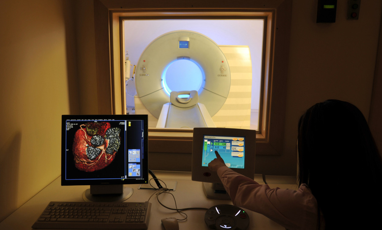
In the lab, the FPGA was inserted directly into a prototype of the final system. The team focused on product validation, bringing up the hardware and software (if needed) in the context of the product’s end application. Any design bugs that slipped through could be tedious to find in the lab. Once one was found, it was a simple matter to reprogram the FPGA and continue bring-up. This serial process worked well as long as the number of bugs remained fairly small.
As programmable chips grew larger and more complex, the number of bugs being found in the lab and the time it took to find them both increased significantly. To keep bring-up schedules reasonable, FPGA development teams realized that they had to do a better job of verifying their designs before going into the lab. In response, FPGA verification teams arose and started looking much like their ASIC cousins.
Register Transfer Level (RTL) simulation remains at the heart of all chip verification, and FPGA teams moved from simple handwritten vector files to more automated testbenches in simulation. Some adopted the constrained-random capabilities of the Universal Verification Methodology (UVM) standard. Static analysis tools for checking clock domains and low-power structures started appearing, and some advanced FPGA teams even began using formal analysis.
More sophisticated verification approaches became more common to reduce the time spent in the bring-up lab and to accelerate time-to-market for the end product. However, FPGA designers still had the fallback position of being able to reprogram a device to fix a bug that slipped through verification and was found in the lab. With the advent of FPGA System-on-Chip (SoC) designs, even this escape mechanism increasingly is unavailable.
The challenges of FPGA SoC verification
Figure 1 shows a representative FPGA SoC, based on publicly published block diagrams from multiple vendors. A large portion of the chip remains traditional programmable logic available for the end product and its applications. However, a hard processor subsystem is included to provide SoC-class power. This subsystem typically includes at least two embedded processors, on-chip memory, and a wide variety of internal and external interfaces.
|
|

There are three reasons why FPGA teams are hitting the verification wall as they move into the SoC era with this type of complex chip. The first is the time to recompile and reprogram a huge FPGA. Once a bug is found and the source RTL code is changed, the process of creating a new image can take an entire day on a high-end personal computer. Then the image must be downloaded to the FPGA, which can take as long as several hours.
Secondly, the process of debug in the lab is also a big factor in the time it takes to make an FPGA design functionally correct. Once the chip is mounted into a real target system, it becomes hard to manipulate inputs or read outputs. Protocol analyzers are available for standard buses, but there are almost always FPGA ports with custom or ad hoc interfaces. It is not at all unusual for a team to spend days or even weeks in the lab trying to track down the source of a single elusive bug.
Depending upon the FPGA architecture, the team may have to make multiple compile/program passes to bring out internal signals for debug purposes. Once the bug is found, it might take even more compile/program passes to try out possible fixes before verifying that the bug has been addressed. Generally, the team will verify the bug and test the fix in simulation before reprogramming. This is a smart move, but adds more time to the debug cycle.
The third aspect of the problem lies in the architecture of the FPGA SoC itself. By definition, an SoC has at least one embedded processor. It may have several, or many, homogenous or heterogeneous processors. The key to an SoC is that the processors are in charge, controlling the data flow between the many functional blocks, memories, and I/O ports. An SoC can do very little without software running on its embedded processors.
The main consequence of this is that some form of software must be available to run on the FPGA SoC’s processors in the bring-up lab. End-product software usually is not ready when the FPGA has been designed, so often the development team has to create special diagnostic software to test the device. This adds a resource burden to the project because this software must be developed in parallel with the hardware design.
Handwritten diagnostic code is time consuming and expensive to develop, hard to maintain, and limited in functionality. Humans are not good at thinking in parallel, so it is rare for diagnostics to stress concurrency in the design, coordinate across multiple threads or multiple processors, or string together blocks into realistic end-user applications. The result is that design bugs may lurk in the FPGA until found at final system integration, or even by a customer.
A solution from the non-FPGA SoC world
To address the diagnostic software code dilemma, FPGA SoC developers must take another page from the book of ASIC and custom chip verification. They can benefit from a method that automatically generates multithreaded, multiprocessor, self-verifying C tests that stress system-level behavior in the SoC. These tests can be loaded into the embedded processor and run in simulation or in hardware acceleration. Figure 2 shows how this method works.
|
|
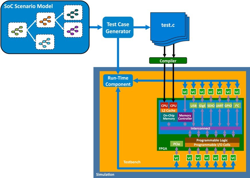
The source for the test case generator is a graph-based scenario model that captures both the intended chip behavior and the verification plan. The generator analyzes the graph to determine the capabilities of the design and then generates a set of test cases that verify these capabilities using the embedded processors. The C code is compiled and downloaded into the processors and run in simulation or simulation acceleration just as any other software would be.
These test cases are designed to stress the FPGA design, running multiple threads on multiple processors in parallel to test concurrent functionality. Since some of the test cases will pull data from the FPGA inputs or send data to its outputs, this approach includes a runtime component in the testbench that coordinates the processors and the I/O activity. It is easy for the verification team to connect to standard UVM Verification Components (VCs).
Creating scenario models is straightforward since they reflect the data flow in the design and resemble SoC block diagrams. This initial investment enables the generation of virtually unlimited test cases to run in simulation. If a suitable connection to the I/O pins is available, it is even possible to run these test cases on the programmed FPGA.
This generation approach provides FPGA developers with a vast improvement over traditional “burn and churn” reprogramming cycles as bugs are found one by one in the lab. Automated test cases save development time, provide more thorough verification, and save resources because embedded programmers don’t have to develop throwaway diagnostics. The result is a faster and more predictable FPGA development schedule for even the most complex SoC designs. Such a test case generator is available today: the TrekSoC solution from Breker Verification Systems.
Breker Verification Systems www.brekersystems.com
Follow: Twitter Facebook LinkedIn Google+ Blog YouTube