Heterogeneous system architecture: Multicore image processing using a mix of CPU and GPU elements
December 01, 2012

Image processing is computationally intensive, requiring immense resources in CPU and memory throughput. Parallelism through multiple CPU cores helps,...
Although multimedia processing has benefited tremendously from the increased availability of multicore processors, until recently, the tendency has been to consider multicore from the standpoint of largely homogeneous CPU architectures. A typical approach offers dual, quad, and higher numbers of cores arranged in Symmetric Multi-Processor (SMP) or cache-coherent Non-Uniform Memory Architecture (ccNUMA) groups. These devices sometimes come with additional hardware acceleration to offload particularly difficult tasks, such as the Context-Adaptive Variable-Length Coding (CAVLC) or processor-intensive Context-Adaptive Binary Arithmetic Coding (CABAC) entropy encoding functions used in H.264 video processing.
Many companies now offer integrated graphics in their devices, largely as a way to save board space and bill of material costs. An additional benefit of having an integrated Graphics Processing Unit (GPU) is that it can provide another path to attacking challenging computational tasks. As an example, AMD’s R-Series processors integrate the Bulldozer CPU architecture with a discrete-class AMD Radeon GPU to produce an Accelerated Processing Unit (APU).
Figure 1 shows a high-level view of the architecture. The GPU is an array of Single Instruction Multiple Data (SIMD) processing elements. Note the common memory controller between the array and x86 cores. This architecture is an early step in the movement to AMD’s Heterogeneous System Architecture (HSA), which breaks significantly from the traditional multicore approach by treating integrated graphics processing elements as a pool of computational resources that can be applied to nongraphics data. It is similar to the way that an attached hardware accelerator can be used, but with the advantage of being a large cluster of programmable devices – up to 384 cores at the high end – with many hundreds of GFLOPS worth of computational throughput.
|
|

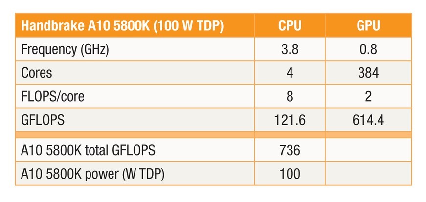
Table 1 illustrates the basic operating parameters of an AMD desktop part with the same underlying architecture as the AMD R-Series APU. The Bulldozer-based CPU’s floating-point performance at 121.6 GFLOPS is dwarfed by the GPU, which offers 614 GFLOPS to applications that can utilize the resource effectively. The key to leveraging the added GPU processors in imaging is to consider the time needed to transfer a block of data to the GPU, process it, then return the results to the main thread.
|
|
Performance analysis in a video transcoding application
Although current-generation AMD R-Series processors require a buffer transfer between the GPU and CPU, data-parallel applications can achieve an improvement in throughput and power efficiency that significantly outweighs the cost of the data transfer.
One example of a data-parallel application is Handbrake, a widely used video transcoding utility that runs on a variety of operating systems and hardware platforms. The utility is notable in that it has well-integrated multicore support and therefore serves as an appropriate platform to study the effectiveness of multicore strategies. Handbrake uses x264, a full-featured H.264 encoder used in several open-source and commercial products that provide adequate multicore support.
OpenCL has been used in both of these projects to maximize the GPU compute resources available within the APU. In x264, the quality optimizations associated with the lookahead function were ported completely to OpenCL on the GPU. This can be used in transcoding applications to improve the output video quality and normally consumes up to about 20 percent of CPU time. Handbrake uses x264 directly as the video encoder. In addition, Handbrake uses OpenCL to perform video scaling and color space conversion from the RGB to YUV color space. AMD’s hardware video decoder (UVD) was also used in Handbrake to perform some of the video decoding tasks.
Data was produced on a Trinity 100 W A10 desktop machine; however, the underlying architecture is identical to that used in the embedded product.
To simplify analysis of the APU’s complex power management architecture, the top Thermal Design Power (TDP) was evaluated instead of breaking out the power consumed by each subsystem. The data displayed in Table 2 shows that when processing is performed purely in the CPU, a 14.8 fps frame rate is achieved, and processing is accomplished in 62 seconds. Involving the GPU and UVD blocks in the processing increased the frame rate to 18.3 fps, reducing processing time and hence power consumption by 14 seconds or 22 percent.
|
|

The floating-point operations total in Table 2 is the product of the floating-point throughput from Table 1 and the processing time, from which can be drawn a figure of merit: operations per watt. Looking at the total floating-point operations and normalized operations per watt, it becomes clear that processing resources are being left on the table. CPU-only throughput is 75 operations per watt, while it is boosted to 353 operations per watt when the GPU is added for an improvement in theoretical floating-point throughput of nearly 5x (4.7).
Twenty-two percent is nontrivial savings, but while this generation of APU makes significant progress in the direction of HSA, all memory accesses are not uniform from the standpoint of latency and throughput. When the kernel accesses memory, it does so directly. Such operations occur at a theoretical rate of 22 GBps or 16 to 18 GBps in typical applications. When a buffer is created in host memory to access GPU data, however, that data goes through a different path where the effective bandwidth is closer to 8 MBps. This means that the gap in memory bandwidth between what the kernel can expect locally and what it can expect if the programmer sets up a local buffer to GPU memory is nearly 3:1. This is symmetrical. If the GPU needed data residing in CPU memory, the same relationship would hold true.
Future devices adhering to the full HSA architecture will have a uniform memory model, eliminating the need to copy data between the CPU and GPU memory regions. Algorithms such as the lookahead functions of x264, when moved into the GPU’s processing domain, will have near parity from the standpoint of memory bandwidth.
Performance analysis in a benchmarking application
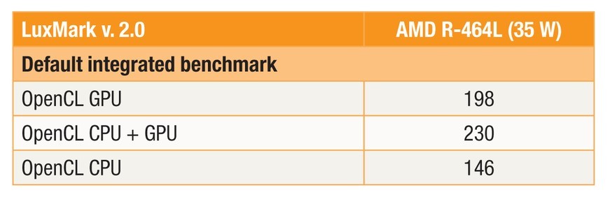
A second example of a data-parallel application is LuxMark, a graphics-oriented benchmarking package that uses OpenCL and illustrates what can be achieved when differences in memory access times are removed from the equation. The default integrated benchmark was run on the AMD Embedded R-464L APU, whose characteristics are shown in Table 3.
|
|

The results in Table 4 clearly demonstrate that the GPU outperforms the CPU by more than 25 percent for this class of processing task. With a full HSA implementation, one would expect to see the addition of the CPU plus GPU to be close to the sum of GPU plus CPU: 344. In practice, the resulting number is 230, which is a nontrivial 63 percent boost but not reflective of fully utilized resources. The gap is largely explained by the overhead of the CPU parsing data and transferring the data back and forth between the CPU and GPU at the lower speeds described earlier. Such features will enable the utilization of both the CPU and the GPU with minimal overhead, allowing the combined performance of both CPU and GPU to be significantly better than either one alone.
|
|
Maximizing computational resources
Newly released APU products provide significant computational resources to designers of embedded computing products. Taking advantage of those resources requires a solid understanding of the underlying hardware architecture, insight into the data flow issues within the target application, and familiarity with the latest tools such as OpenCL.
AMD www.amd.com
Follow: @AMDembedded Facebook Linkedin YouTube