
Configurable A/D Peripherals Overcome the Shortcomings of SoC Devices
March 01, 2013
Blog

The microcontroller selection process often occurs before a design is finalized and while features are being changed on a frequent basis. This makes s...
One of the most frustrating scenarios for embedded system designers occurs when, after they’ve completed many design milestones, they discover that the embedded device initially chosen does not meet the current design requirements. During the course of the development cycle, requirements change and other unforeseen challenges occur, especially with a new product design.
System-on-Chip (SoC) devices, especially mixed-signal SoC devices, have been developed to overcome these difficulties. While different SoC companies have varying ways they like to describe their SoCs, in the end, an SoC is essentially a microcontroller (whether it be a low-power 8 bit or a high-power 32 bit) with a large number of integrated analog and/or digital peripherals. Additionally, SoC devices introduce the ability to customize, configure, and program these resources.
Configurability allows customers to have flexibility as to how peripherals such as comparators and operational amplifiers are routed out to pins. These components will not have the same static pin locations as a traditional fixed-function microcontroller. Using a series of registers on the device, customers can configure a device to their particular application needs. Additionally, mixed-signal SoC devices may also contain digital resources that are programmable at different levels, from basic configurable logic to larger Programmable Logic Device (PLD) resources that can be configured using a hardware description language such as Verilog. Using these programmable digital resources, developers can easily create state machines and other complex circuits, such as performing an FFT on a digital signal in hardware.
While having this high level of configurability allows developers to accommodate design changes that may occur during development, there are still some instances where the limitations of the chosen SoC are reached. These limitations can arise from the design requirements exceeding the capabilities of the part or by the need to implement a feature or specific functionality that does not have a fixed-function component on the device silicon. By utilizing the configurability and flexible routing that make using a mixed-signal SoC so useful in the first place, developers can overcome many of the shortcomings the device architecture itself may have. Exploring several of those design challenges and a few practical examples of how an SoC device can overcome those issues lends insight. These techniques can often allow design requirements to still be met without the need to change the SoC device currently used in the design.
Overcoming analog SoC challenges
Overcoming analog design challenges can be one of the most difficult things in embedded mixed-signal development. Unlike digital peripherals, which are considered to be more “universal” and act more like building blocks, analog peripherals are “fairly fixed” in their functionality as they are essentially a system of components themselves rather than building blocks. Engineers will have access to analog peripherals such as Analog-to-Digital Converters (ADCs), comparators, and Digital-to-Analog Converters (DACs), all of which can be configured to some level.
One design challenge that is commonly faced is the need for an additional ADC in a design. This can be encountered in the instance where a customer does not want to multiplex an ADC input or would like to implement a specific type of ADC, such as a Successive Approximation Register (SAR) ADC in a device that only contains a Delta Sigma ADC. To understand how an SoC can overcome this from within itself, let’s look at this from the perspective of needing a SAR ADC in a design. The components required to build a SAR ADC are a comparator, a DAC, a status register, and some programmable digital logic. All are components that can be found on SoC devices. When these components are arranged in a fashion that is similar to that shown in Figure 1, a functional SAR ADC can be created.
|
|

The 8-bit output is gathered by reading what is stored in the Status Register. Various digital functions, such as arithmetic operations and bit shifting, are done in hardware using Verilog. This combination of resources has created functionality that did not previously exist in the device that is capable of 118 KSps at 8 bits. As an additional benefit, as long as there are more comparators, DACs, and digital logic, additional SAR ADCs can be provisioned.
Many mixed-signal SoC devices also contain dedicated comparators and operational amplifiers. When those resources become exhausted or, in the case that the device never included those peripherals from the start, what can be done? Analog circuits, such as comparators, active filters, programmable gain amplifiers, and transimpedance amplifiers, all are comprised of an operational amplifier that uses various resistors and/or capacitors to create a specific function. Some mixed-signal SoCs contain what are called Switched Capacitor (SC) peripherals. SC peripherals are built around low-noise, low-offset op-amps surrounded by analog multiplexers that are surrounded by groups of capacitors and switches. If the switches are put into a static open or closed state, then the result is a capacitor attached to the circuit. In addition, if the switches are opened and closed alternatively at a certain frequency, then the switched capacitor begins behaving like a lossless resistor.
Devices that incorporate switched capacitors, such as the PSoC family of devices from Cypress Semiconductor, use register configuration to control the switches in the switch capacitor topology to produce a variety of circuits, from the most basic of operational amplifier to more advanced circuits such as a mixer, integrator, or tack and hold.
Overcoming digital SoC challenges
Developers face significant digital design challenges with SoC architectures. Considering a traditional microcontroller, it will contain some fixed-function digital peripherals such as Pulse Width Modulators (PWMs) and timers. SoC devices incorporate digital logic, such as programmable logic devices, Arithmetic Logic Units (ALUs), and Status/Control resistors. Using hardware description languages such as Verilog, these hardware resources can be configured to work together to create many possible functional components.
Consider an SoC device that contains a peripheral USB interface. Late in the design cycle, it is decided that it would be beneficial to also support host USB capabilities for features such as allowing a USB flash drive to be connected for data logging or field programmable firmware updates. The problem is that the device being used does not contain the required hardware to implement host functionality. However, using the configurable digital resources, an SoC device can overcome this digital design limitation.
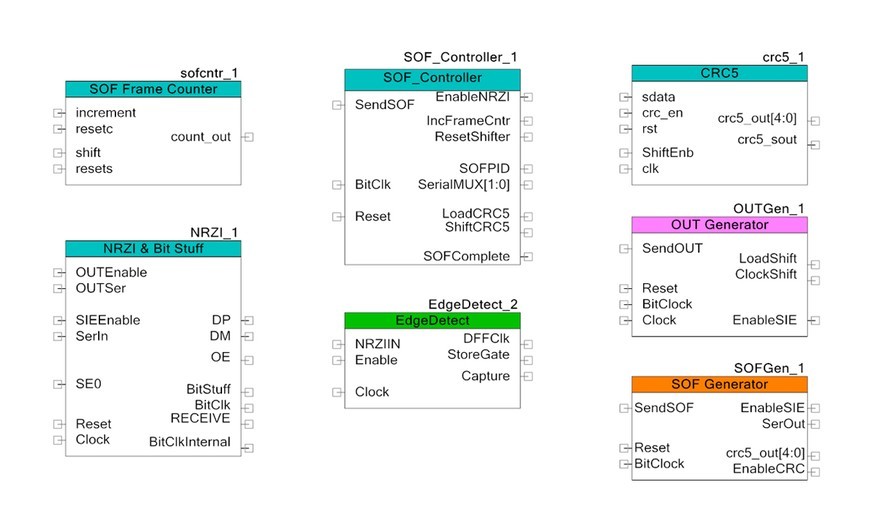
To understand what needs to be incorporated, think about what it takes to handle USB communication. There are the differential signals, then SOF generation, Non-Return-to-Zero Inverted (NRZI) encoding/decoding, Cyclic Redundancy Checks (CRC) calculating, bit stuffing, and IN/OUT packet parsing. If designers read the USB specification, they will see that everything required can actually be implemented in a PLD, along with the help of some additional components. With some extensive Verilog coding to utilize the digital resources previously described, individual components for host USB communication can be made as shown in Figure 2. Here, each block shown represents Verilog implementation with various digital inputs and outputs. By connecting these components together with some glue logic, along with the addition of some external pull-down resistors and a crystal oscillator, a fully functional USB host can be implemented.
|
|
Such configurability means that if a mixed-signal SoC is selected for a design that contains, for example, two PWMs, two comparators, two DACs, and one Delta Sigma ADC, these peripherals are not the end of its hardware functionality. Resources can be repurposed and modified to extend resources to functionality that is different from what might have been initially required. In this way, engineers can increase the value of a product as well as reduce development time of a new product design without having to migrate to a new embedded device; that decision often leads to new firmware development and PCB layout, resulting in lost time and money. By calling upon skills learned in early electrical engineering classes combined with the flexibility of a mixed-signal SoC device, embedded systems designers can efficiently compensate for the shortcomings of their SoC designs.
Cypress Semiconductor www.cypress.com/?id=1353
Follow: Twitter Blog Facebook Google+ LinkedIn YouTube


