
FPGAs for embedded AI: Reducing power consumption, programming complexity for mass markets
June 19, 2018
Blog

Developers are investigating AI in embedded applications for automotive, industrial, and consumer markets. Many of these have strict thresholds in terms of the power consumption and complexity.
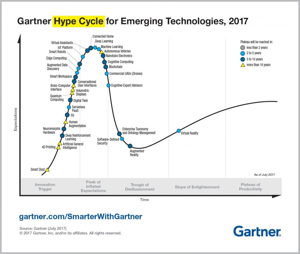
It’s official. The hype torch has been passed from the Internet of Things (IoT) to artificial intelligence (AI). But for engineers getting acquainted with machine learning, deep learning, and other AI enablers – or, for that matter, anyone familiar with the Gartner Hype Cycle – AI is on a collision course with the Trough of Disillusionment (Figure 1).
There are many market dynamics at play in a technology’s nosedive into the Trough, including sensationalist marketing, excitable media, and even over-engineered concepts from smart designers who forgot to consider the business case. However from a technical standpoint, what will accelerate AI’s fall from grace is power consumption and programming complexity.
I’ve written previously on processor power consumption in AI-enabled embedded systems, and since then the wide range of real-world AI use cases has become clearer. Today, developers are investigating AI in embedded applications for the automotive, industrial, commercial, and consumer markets such as key phrase recognition, face and object tracking, object counting, and traffic sign detection to name just a few. Many of these functions don’t require the operations per second (OPS) performance provided by the processors I covered at the time, but do have strict thresholds in terms of the power consumption, size, and cost they can add to an overall system design. Focusing on power specifically, compute solutions responsible for these tasks often need to fit in 1 W (or even sub-1 W) envelopes. This is a significant design hurdle, especially considering many off-the-shelf CPUs, GPUs, and DSPs that target AI edge processing struggle to come anywhere close to those levels.
Shrinking power consumption for AI edge enablement
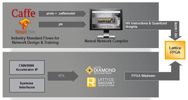
It’s common that technologies originally designed for one purpose are also well suited to others, which is the case with FPGAs for deep learning workloads. Lattice Semiconductor, for example, has a legacy of delivering glue logic and interface FPGAs into low-power edge systems, and realized those solutions could be repurposed for flexible, sub-1 W AI inferencing applications. This is now possible with the company’s sensAI technology stack (Figure 2).
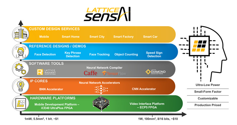
The Lattice sensAI stack is based on the ICE40 UltraPlus FPGA and ECP5 FPGA, which enable the creation of Binarized Neural Network (BNN) and Convolutional Neural Network (CNN) accelerators, respectively (Figures 3A and 3B). The stack also includes software development tools, hardware development platforms, reference designs, and an onramp to third-party design centers to help accelerate the deployment of high-volume consumer and industrial machine learning systems.

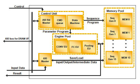
Figure 3B. As part of Lattice Semiconductor’s sensAI technology stack, the ECP5 FPGA is optimized for use as a more robust Convolutional Neural Network (CNN) accelerator.
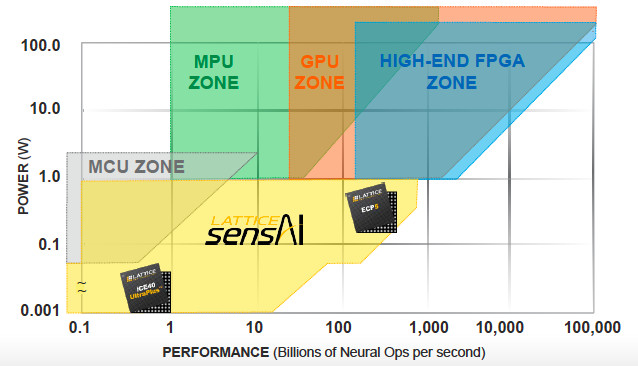
ECP5-based CNN accelerators developed using the sensAI suite support 1-, 8-, and 16-bit resolution for more complex neural networks that require more than 100 billion neural operations per second of performance at less than 1 W of power consumption. Meanwhile, less-demanding BNNs that rely on single-bit quantization and need fewer than 100 billion neural operations per second can leverage sensAI designs based on the ICE40 UltraPlus that consumes between 1 and 10 mW of power (Figure 4).
Cutting complexity for FPGA/AI developers
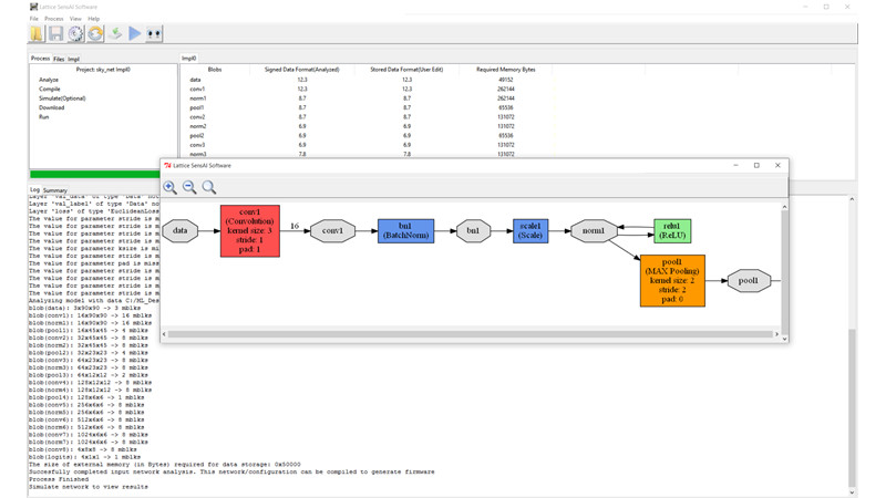
The sensAI stack is supported by the Lattice Diamond and Lattice Radiant software development tool suites, which allow FPGA design engineers to get started with the sensAI stack quickly. For developers who aren’t familiar with RTL or FPGA programming, sensAI also includes a Neural Network Complier that takes the output from deep learning development frameworks such as Caffe or TensorFlow and uses it to help generate a bitstream for the target FPGA. No prior RTL experience is required (Figures 5A and 5B).
The sensAI stack targets applications such as face detection, key phrase recognition, face tracking, object counting, and speed sign detection. However, Lattice recognizes that in many instances its FPGA solutions will be used for pre-processing in systems that also include a higher performance processor.
FPGA SoC devices such Xilinx’ UltraScale+ family have become popular in AI system designs for their reconfigurability and low performance per watt (PPW) when compared with competing higher end architectures. Still, programming these devices remains challenging for developers who are new to FPGA designs, especially when legacy codebases have to be migrated to FPGA SoC designs that support machine learning.
To shorten the development cycle, Silexa recently integrated capabilities in its SLX development tool that refactor C/C++ code for FPGAs into a high-level synthesis-compatible (HLS-compatible) format, and also insert any pragmas needed to account for hardware and software dependencies on heterogeneous multicore SoC targets. Automatic legacy code partitioning, code guidance, and algorithmic exploration features also help accelerate the process of migrating and optimizing code for devices such as the UltraScale+ family before tools such as SDSoC and Vivado are used (Figure 6).

Silexa developed the new SLX features in conjunction with Ricoh and other customers working on sensor fusion and deep learning solutions for the industrial and defense markets.
Embedded solutions serve the AI industry
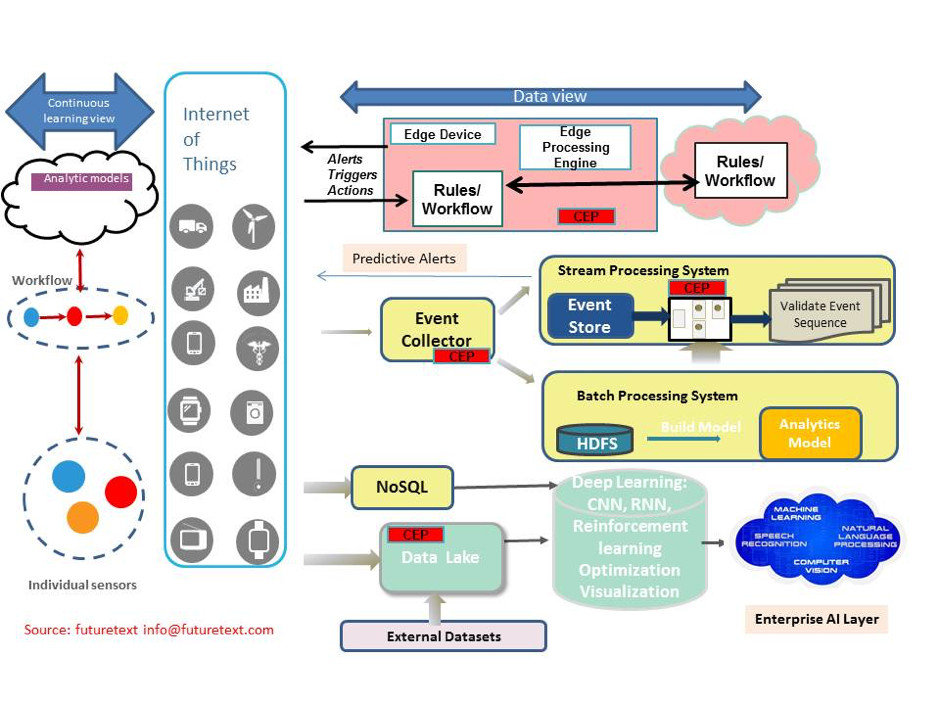
It should be noted that AI technology, in many use cases, is intrinsically mapped to IoT architectures.
As shown in Figure 7, large AI learning models are developed in the data center (cloud), and those models are then condensed into engines or algorithms small enough to run on edge devices. Edge devices use these condensed learning algorithms to draw conclusions about their surroundings (known as inferencing), such as whether an animal is a cat, dog, or human or if a rise in dew point indicates an incoming storm. Over time, these inferred findings can be aggregated back in the data center to continuously improve the AI learning model, which results in more precise learning algorithms, and so on. Therefore, the more systems feeding AI inferences into this virtuous feedback loop, the better.
Why does this matter? Because it makes AI power and programming everyone’s problem.
Fortunately, embedded AI vendors are working out the answers.


