Shunt versus series: How to select a voltage-reference topology
June 24, 2015

When designing a system for applications ranging from automobiles to simple temperature measurements, interfacing with the analog world typically requ...
When designing a system for applications ranging from automobiles to simple temperature measurements, interfacing with the analog world typically requires data converters (digital-to-analog and analog-to-digital), sensors, or other application-specific integrated circuits (ICs). Accurate measurements require a reference voltage that does not fluctuate with system conditions such as input voltage or ambient temperature. A voltage-reference IC provides the steady voltage other ICs use to make measurements with the required accuracy.
There are two types of voltage references: shunt references and series references. Selecting a reference topology for a given application can feel overwhelming. Comparison tables (Figure 1) are a good reference, but do not tell the whole story. In this paper, I describe the applications of both shunt and series references, and what makes each a strong candidate in a given application.
|
|

Shunt
A shunt voltage reference only requires two terminals and is functionally similar to a Zener diode where the voltage drop across the device is constant after reaching a minimum operating current through the device. Figure 2 shows a typical current versus voltage curve for a Zener diode, where VZ is the Zener voltage when reverse-biased by a current of IZ.
|
|

Figure 3 is a basic schematic of a shunt voltage reference.
|
|

The shunt reference in Figure 3 regulates the reference voltage by acting as a variable current sink, effectively creating a variable resistor divider with RS to provide a constant voltage at the output node. The external resistor, RS, is required for regulation, but there is no maximum input-voltage rating for a shunt reference. The resistor sets the total current sourced by the input supply as a function of the supply voltage. The total supply current is the sum of the load current and operating current of the shunt reference.
The input supply, VDD, always sees the maximum load current determined by the input-voltage level and external resistor. The shunt reference also sinks more or less current as the current requirements of the load change. The shunt is effectively acting as a current-controlled current sink, where the load current determines the current that the part sinks from the input supply. In this respect, the shunt reference is always on, and cannot be put into a sleep or shutdown mode.
An increase in input voltage results in an increase in current through the external resistor, and more current is shunted across the reference device. An external resistor prevents the shunt current from exceeding the maximum operating current, IQ_MAX, while also maintaining the minimum operating current through the device, IQ_MIN, under light loading conditions.
Two loading-condition extremes can help calculate the resistor value. The first loading condition is when the input voltage is at its minimum and the load current is at its maximum. The voltage drop across the resistor is smallest when VIN is closest to VOUT. The value of RS must be low enough for VIN to source enough current to meet the demand of the load and still provide IQ_MIN to the reference. The calculated resistance represents the maximum value of the resistor while maintaining IQ_MIN at ILOAD_MAX and VIN_MIN, and is represented as RS_MAX.
At the other extreme, the resistor must be large enough to prevent the operating current from exceeding the maximum current through the reference device, IQ_MAX. When the input voltage is at its maximum and the load current is at its minimum, the current through the shunt reference will be the largest for the application. The resulting resistance from the second calculation is the minimum resistance that still meets the second loading extreme, represented as RS_MIN. For the resistor to be able to keep the device operating throughout all loading conditions between these two extremes, RS_MIN must be smaller than RS_MAX.
For example, an industrial application requires a 2.5 V reference voltage. The system input-voltage supply ranges from 12 V to 48 V and the load device draws between 0.1 mA and 1 mA. The LM4040 2.5 V is an example of a shunt reference voltage for this application, with a minimum operating current of 60 µA and a maximum operating current of 15 mA. You can calculate the external resistor using Equations 1, 2:
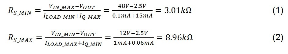
In this example, RS can be any value between 3.01 kΩ and 8.96 kΩ. A higher resistor draws less current from the input supply.
Table 1 shows the total supply current and shunt current for the different loading conditions with two different values of RS, selected as 1 percent resistors near RS_MIN and RS_MAX, respectively. Note that you must calculate both RS_MIN and RS_MAX to ensure that a single resistor can meet all loading conditions, and that RS_MAX is larger than RS_MIN.
|
|

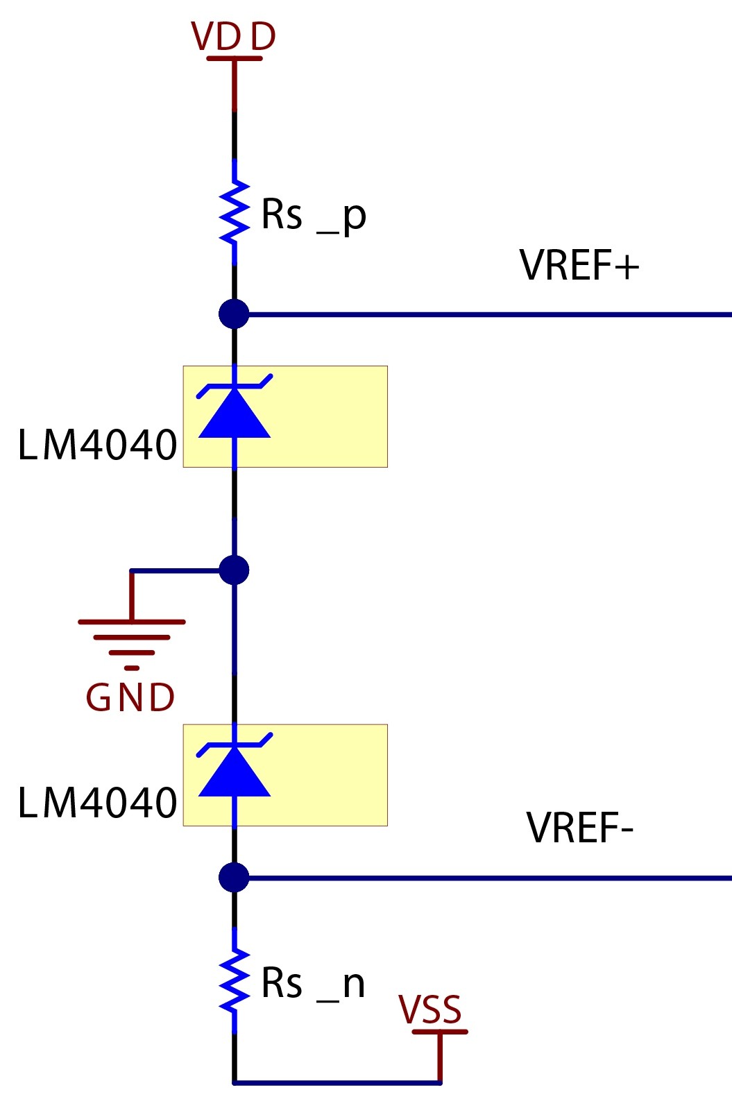
Shunt references are flexible because they can create a floating reference (voltage not referenced to ground) as well as negative references. To use a shunt to create a floating reference voltage, simply use the shunt as described. However, connect it to a lower potential in the circuit instead of connecting the second terminal to ground (Figure 4), where V2 marks the lower potential. To use a shunt as a negative reference, the procedures and calculations remain the same, except RS is connected from the negative supply rail to the ground terminal of the reference. The output is between the resistor and the ground terminal, and what was the input terminal is now grounded (Figure 5). A typical application for a negative voltage reference is a bipolar data converter, such as a digital-to-analog converter (DAC), which requires positive and negative references to generate the full range of possible output voltages. Figure 6 shows an example using two shunt references in a bipolar reference configuration.
Floating reference
|
|

Negative reference
|
|

Bipolar reference
|
|
Series
The second type of voltage reference device is a series voltage reference. A series voltage reference requires three terminals: VDD, VOUT and GND connections. Figure 7 shows a series voltage reference device that does not require an external resistor. It only consumes as much current as required by the load, plus a small quiescent current. Therefore, the input supply sees a decreased load and a decrease in power consumption when the load is not using as much current.
However, the series device does have a maximum-rated input voltage, and is not easily configured for floating or negative references.
|
|

The input voltage of a series voltage reference must be at least the output voltage plus some device-specific dropout voltage, and must not exceed VIN_MAX. The dropout voltage is the minimum voltage difference between VIN and VOUT for that device under a given load, and is stated in the device datasheet.
A series voltage reference also allows for additional functionality with extra pins on the device (for shutdown or sleep) to limit power drawn from the input supply. This power savings is advantageous in applications such as a mobile device, where battery life is critical. If the load device does not always need to be enabled, the series voltage reference can be disabled by controlling the EN pin. Figure 8 is a schematic of such a series voltage reference.
|
|

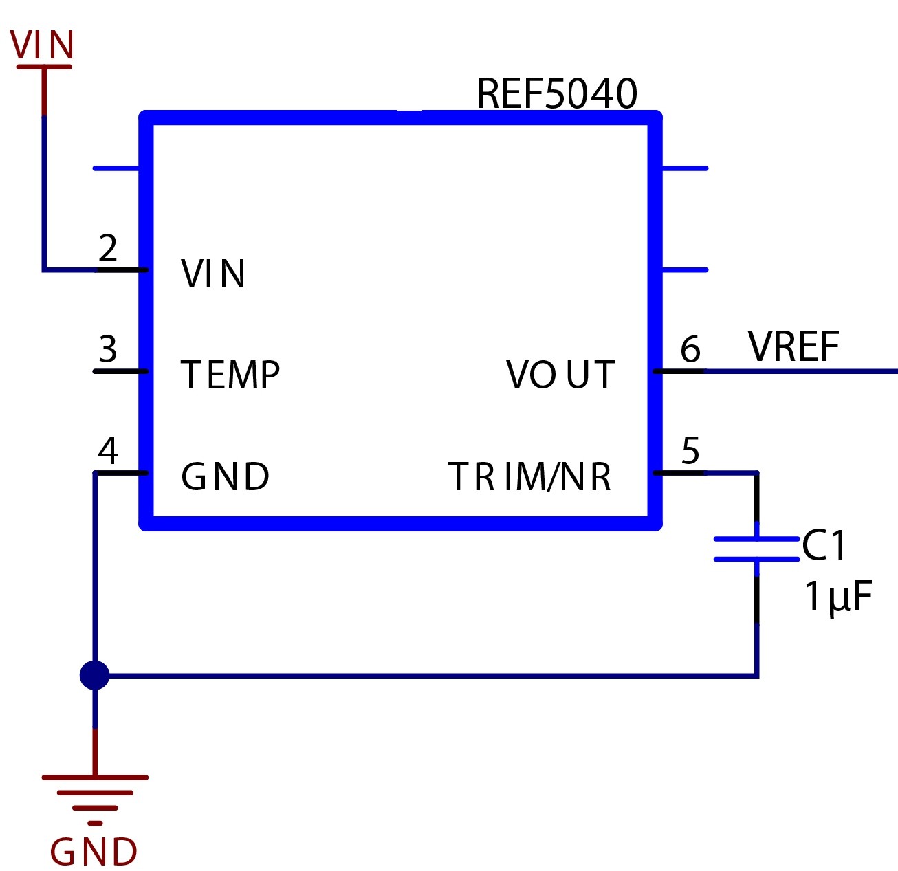
Another feature that uses an extra pin offers the ability to fine-tune and trim the reference voltage with external resistors. This feature can also reduce noise with a capacitor using the TRIM/NR pin on series voltage references, such as the REF5040 and the rest of the REF50xx family. This family of devices also has a TEMP pin to approximate device under test (DUT) temperature. Figure 9 shows a schematic of this series voltage reference with a 1 µF noise-reduction capacitor from the TRIM/NR pin to ground.
|
|
As an example of using a series voltage reference to take advantage of the potential power savings, let us say you need a voltage reference in a mobile application where power consumption is a concern. The load device draws 1 mA for 1 second, followed by 10 µA for 9 seconds, but the reference must be enabled at all times, so both a shunt and series reference are possible choices. The system is powered by a small coin-cell battery with 25 mAh capacity and a nominal output voltage of 3 V. The series reference is can be used for this application because the input voltage to the reference will not exceed the reference’s maximum input voltage, and the battery will see reduced loading 90 percent of the time.
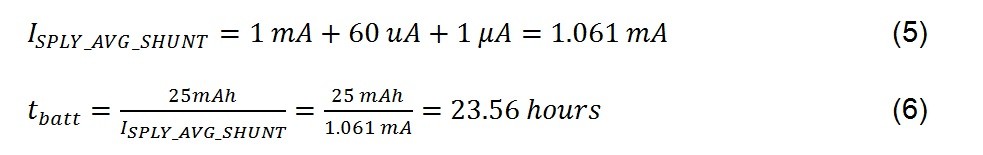
The LM4128 series reference has a typical operating current of 60 µA. The load device is controlled by a microcontroller, which is also powered by the battery, but the microcontroller is only active when switching the state of the load device and therefore draws an average supply current of approximately 1 µA (derived from MSP430G2001). To approximate battery life, divide the total capacity of the battery in milliamp-hours by the average load on the battery. In this case, the operating current of the reference is added to the load current, along with the supply current of the microcontroller, to calculate the average load on the battery (Equations 3, 4):


Using our shunt voltage reference device for example, the supply current is fixed and does not change with the demand of the load, since excess current is shunted to ground through the reference. In this example, the battery would always supply 1 mA plus the shunt-reference operating current (shown as 60 µA for comparison), plus the 1 µA draw of the microcontroller (Equation 5. 6):
The system with the series reference will consume much less power compared to the shunt reference, and subsequently last longer in a mobile, battery-powered application. Several factors can affect battery life, but this simple example shows the difference in power consumption between series and shunt voltage-reference operation.
Conclusion
Some key pieces of information to know when choosing a voltage reference include:
• The input-voltage range, including the need to tolerate wide-input voltage swings.
• The total load seen by the reference and whether the load is fixed or variable.
• Whether the load is always present; and if not, if the reference can be shut down.
• The reference polarity and whether negative references are required.
A shunt reference is a good choice when the load current is known to remain fairly stable and the system has a wide-input voltage range. The selection of external resistor is important, but does not have to be complicated. A shunt reference is also great for creating multiple, stepped reference voltages on a single-voltage input, or when you need to quickly and easily create positive and negative references.
A series reference is best when the load current may change often, while the input voltage is fairly constant and within the bounds of the device limits. The enable and disable functionality of a series reference offers the potential for significant power savings, and the TRIM/NR pin adds additional flexibility.
Now that I’ve covered the initial selection criteria of shunt and series references, the next step is to understand the specifications and how they contribute to error. This is covered in the “Voltage Reference Selection Basics” white paper.
References
1. Download these Texas Instruments datasheets: LM4040, LM4128, REF5040, MSP430G2x01
2. Endo, Mario. “Voltage Reference Selection Basics,” Texas Instruments White Paper (SLPY003), June 2014
Additional links/tools
1. TI voltage reference site
2. Voltage reference product overview
3. WEBENCH® series voltage reference selector tool
4. Reference designs
5. Dean, Christopher. “Understanding voltage references: Shunt vs series. Which topology is right for you?” Texas Instruments Precision Hub blog, April 29, 2015