MEMS & Sensors packaging: The challenges ahead
September 22, 2015

MEMS & Sensors devices have infiltrated our daily lives, having found their way into a broadening variety of applications from smartphones to cars, wi...
MEMS & Sensors devices have infiltrated our daily lives, having found their way into a broadening variety of applications from smartphones to cars, with millions more uses in between. Applications are becoming increasingly diverse in nature, and each has its own unique specifications, especially when it comes to the required sensor type, such as barometer, gas, humidity, and so on. As MEMS & Sensors technologies have moved beyond automotive applications into consumer and mobile devices, the outsourced assembly and test (OSAT) community has sought alternative, more cost-effective packaging solutions for customers. Specific materials, including die attach or mold compound, were co-developed with material suppliers in order to provide more economically advantageous and size-effective solutions. The first wave included mainly inertial devices, but now there are many optical and environmental applications popping up and looking to fulfill the “magic” triptych: smaller footprint, lower cost, and higher performance.
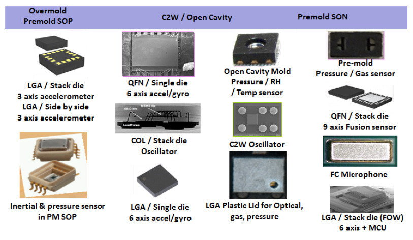
A sampling of MEMS & Sensors
Original MEMS & Sensors IDMs are still in a very strong position, but with many new players entering the market, thanks to innovative concepts inspired mainly by the fabless model, OSAT players are being driven to constantly innovate in order to serve complex customer-specific requirements. Additionally, they are attempting to keep some commonality between the different platforms that exist. The IDM community is likewise challenged as it is becoming harder to invest in multiple packaging solutions while staying ahead of the curve in terms of product innovation and time-to-market. Some IDMs increasingly rely on OSAT partners to package high-volume consumer devices with the manufacture of automotive and industrial devices remaining firmly in-house.
Today, the hype around IoT is becoming louder, and the reality is that complex challenges lie ahead as far as MEMS & Sensors packaging is concerned. Design engineers seek enhanced software, greater connectivity, and sophisticated hardware. Hardware is increasingly becoming a solution enabler, and this is putting even more stringent requirements on price, footprint, and power consumption. Wearable devices are driving device thickness down significantly, in addition to power consumption and price. However, the main challenge does not concern MEMS & Sensors packaging itself; instead, the main challenge is for the OSAT community to effectively deliver the most suitable architecture to fulfill module and/or SiP integration. Are future MEMS & Sensors solutions going to package bare die in a SiP, or, will MEMS & Sensors be integrated in a packaged format? If large IDMs have the strength and capability to provide the majority of components for their subsystems, they will drive their own strategies. However, for other players, MEMS & Sensors packaging will become critically important. Based on current smart module solutions currently available on the market, significant size and consumption reduction is possible to achieve, especially if system, device, and package players collaborate consistently and openly during the early stages of product development.
With the overall need for advanced functionalities in devices, business direction is driving the OSAT community to propose new and diverse package solutions that will help customers find the most suitable solution in terms of:
- Performance (electrical & mechanical)
- System integration
- Time to market
- Cost
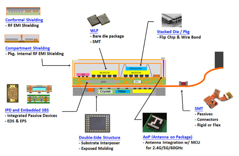
With more and more stringent specifications emerging for footprint and device height for wearable applications, 3D wafer level package (3D WLP) with through silicon via (TSV) is definitely a solution that will enable further smart integration for MEMS & Sensors. 3D WLP is emerging as a “must have” technology for wearable and medical applications; however, other applications serving smart home and industrial markets will likely count on more “classical” platforms. But these are not without their own unique set of challenges. As such, the OSAT community is trying to offer all the key building blocks to provide the smartest system integration, regardless of application.
One area poised to see significant growth for the MEMS industry is that of medical applications. While many applications have already been introduced to the market, in reality we are merely seeing the tip the iceberg. Not only will the medical profession further adopt technology for the practice of healthcare and sick care, but broader society will increasingly use technology to track wellness and fitness in everyday life. MEMS will play a major part in all these applications. There are four main groups that can be distinguished: biosensors, bio MEMS for diagnostic (disposable or portable), on skin or swallowed devices (treatment tracking, etc.), and, finally, permanent-implanted MEMS. The first type (biosensor) is now lined up to be widely deployed in many products, especially fitness bracelets, smart watches as well as smartphones, to track several vital signs (like the example from Leman Micro Devices) and activity trends. The example below is a small module typically integrated in the smartphone that can monitor up to six vital signs. By combining advanced assembly technologies, it is now possible to combine multiple ICs with optical and mechanical sensors, MEMS, and passives in a single module that can fit within a smartphone or in a wearable device. Diagnostic applications will benefit from biosensor developments, but one of the main roadblocks today is the microfluidic part, which is often needed for such devices.
The road ahead for ingested devices or implantable devices is still paved with major obstacles. Bio-compatibility, self-power, and very high reliability (especially implant) are key elements. Today, some niche and fragmented devices are available, but we are still far from large-scale deployment.
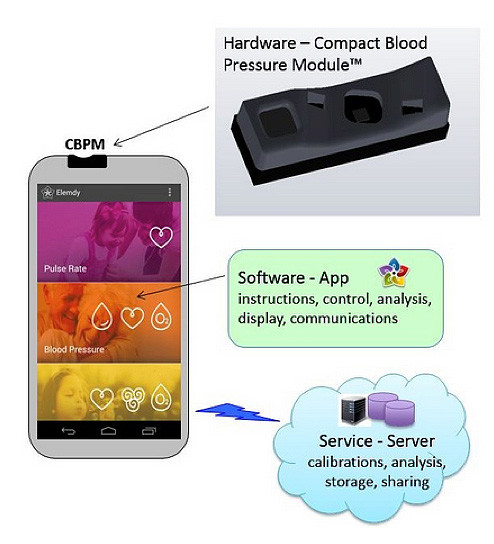
Courtesy of Leman Micro Devices
Regardless of the specific platform that is chosen for these future applications, it has become clear that the MEMS industry is well-positioned for the future. With a wide range of solutions to choose from – both advanced and classical – MEMs will continue to play an important role in the future of consumer devices, medical devices, and automotive applications. While it is hard to speak to the overall market growth, it’s clearly evident that the demand for solutions is increasing year after year.
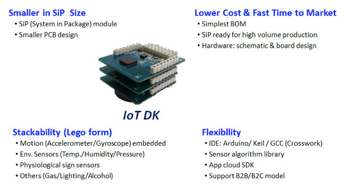
Smart module and/or SiP integration is key and will allow large deployment of connected devices. To do so, early collaboration between the different players within the value chain is important, as well as a simplified supply chain. System integrators have to develop and propose design kits, so end customers can easily evaluate different system configurations before designing a specific module or SiP. (The following IoT design kit from ASE Group serves as an example).
Christophe Zinck is Senior Application Engineering Manager at ASE Group.