
Manufacturing MEMS to the quality standards of multiple industries
June 21, 2018
Blog

Although the promise of MEMS is only starting to be tapped, the challenges of manufacturing MEMS are daunting because the category covers so many different types of devices.
Microelectromechanical systems (MEMS) are devices made in specialty microelectronic fabs that combine electronic functions and mechanical actions. MEMS, as a technology platform, have enabled the manufacture of unique sensors and actuators that act as eyes, ears, nose, tongue, and even organs. Although the promise of MEMS is only starting to be tapped, the challenges of manufacturing MEMS are daunting because the category covers so many different types of devices, used in a wide variety of industries that each present unique standards and technical demands.
MEMS technologies are characterized by custom designs, often with features that have high aspect ratios (i.e, tall, skinny, and fragile). Many of these devices are used in harsh environments that present demanding thermal conditions and mechanical stress. While the manufacturing of MEMS devices is similar in ways to the manufacturing of integrated circuits, MEMS, in general, use less-conventional materials and have a much wider variety of functions. The form factors of integrated circuits tend to fall into only a few basic categories, while MEMS devices take a much wider variety of forms, including accelerometers, gyroscopes, pressure sensors, printer jets, display devices, microphones, and many others.
Because the applications and form factors for MEMS vary so greatly, manufacturing them to high standards of quality is exceptionally challenging. This article examines a specific application of MEMS and how, through utilizing a disciplined quality system approach, high yields and consistent delivery can be achieved.
For example, One particularly challenging product Sensera manufactures is silicon dies containing thousands of micropillars – in this case, tiny pillars about 6 µm in diameter (roughly 1/10th the thickness of a human hair) and 40 µm tall (Figure 1). These dies are used as molds to manufacture polymeric membranes. The membranes are employed in microfluidic devices that are used for an organ-on-a-chip application to better understand human biology.
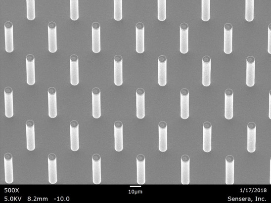
[Figure 1 | Scanning electron microscope (SEM) picture of micropillar structures at 500X magnification.]
As described by Dr. Richard Novak, Senior Staff Engineer at Harvard University’s Wyss Institute for Biologically Inspired Engineering, “These microchips, called ‘organs-on-chips’, offer a potential alternative to traditional animal testing. Each individual organ-on-chip is composed of a clear flexible polymer about the size of a computer memory stick. The polymer contains hollow microfluidic channels, which are lined by living human cells. The channels interface with artificial veins, which are also lined with human cells. Mechanical forces can be applied to these channels to mimic the functions of living organs, including breathing motions in the lung and peristalsis-like deformations in the intestine.”
As simple as the task of spacing micropillars evenly in a die might seem, it presents numerous manufacturing difficulties. For a start, these high-density, high-aspect-ratio features are brittle, and easily broken by the slightest contact. Because the pillars are a feature of the die used to create holes in the polymeric membranes (Figure 2), broken pillars will result in missing holes in the membranes, consequently blocking the desirable cellular exchange in the organ-on-a-chip. Additionally, broken pillars will become debris that, if displaced and reattached, will risk damaging other pillar areas. We must be extremely careful when handling these dies to guarantee the integrity of the micropillar array.

[Figure 2 | The micropillar die (upper right) creates the holes in the polymeric membrane (lower left image courtesy Wyss Institute).]
In addition, these thousands of micropillars are like a magnet for dirt and particles. In fact, micropillars are used in some dust-removal devices specifically because of their dust-attracting properties. In a MEMS device, any tiny dust particle, clothing fiber, or contaminants from skin or hair will lead to defects resulting in unusable devices.
That leads to one of the biggest challenges when manufacturing these parts: compliance with tight defect criteria. These tight defect criteria are necessary because organs-on-a-chip are employed in research projects with human blood, which is wasted if used in defective devices caused by defective molds. Furthermore, accurate testing devices are necessary to ensure accuracy and repeatability of the results.
Another challenge when manufacturing these devices is to meet the tight dimensional criteria of the pillars. Any instability or slight shift in process conditions will lead to large shifts in pillar dimensions which, as well, will result in device failure.
Implementing a stringent quality management system (QMS) was the most helpful in overcoming and continuing to overcome all these challenges. The QMS focuses on continuous improvement of processes and systems, constant analysis of risk and opportunities, and preventing non-conformities. The QMS is implemented from the moment a purchase request for materials is made. It continues through the whole manufacturing process, and concludes only when the product is shipped to the customer.
The most important element of the QMS is constant monitoring of even the most minute aspects of the production process. During and after photo processing, for example, the photoresist coating tool performance, the photoresist critical dimensions (CDs), and the wafer cleanliness are monitored and real-time records are kept.
Within the statistical process control charts and traveler process control plans (Figure 3), Sensera sets not only upper specification limits (USL) and lower specification limits (LSL) within which measurements need to be, but also upper control limits (UCL) and lower control limits (LCL). Continually monitoring these control limits allows for the identification of trends and small drifts in key process parameters, so they can be corrected.
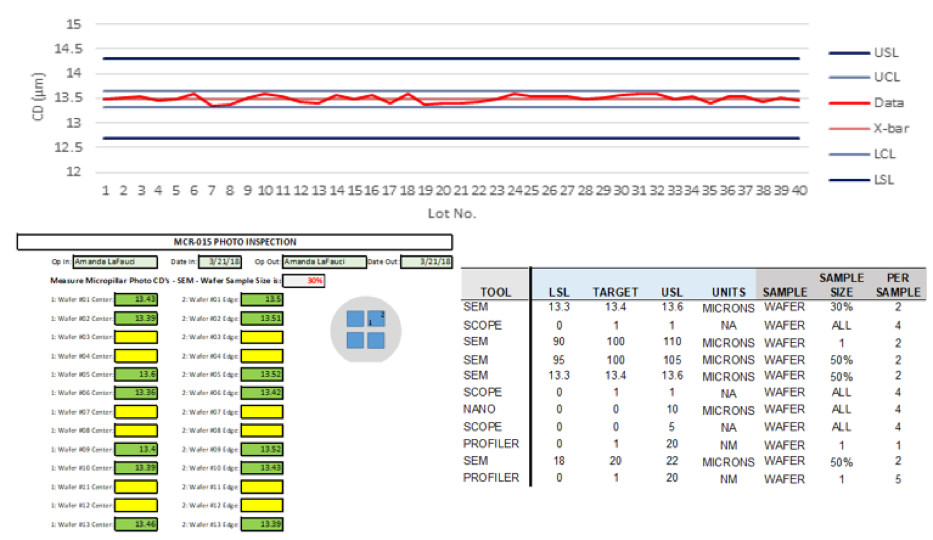
[Figure 3 | Examples of statistical process control charts (top) and traveler process control plans (bottom).]
Monitoring the production process so intensively, in such detail, may seem almost obsessive, but we have found it necessary in order to maintain the microscopic accuracy necessary for MEMS manufacturing. This quality control process has improved Sensera's yield by 20 percent.


